On-delay time relay based upon the 555 timer (includes the PCB)
What is it?
An On-delay time relay is a device that activates its load after a time has elapsed; that is, the load is not activated immediately when you apply power to the relay, but at a programmed time afterwards.
In my article about avoiding cold start in our electronic circuits I explain that when the capacitors in a power supply are completely discharged they behave like a short circuit when you apply power for the first time; this short circuit can propagate to the delicate components of your circuit, damaging them. Ideally, your circuit should not receive power until the capacitors have fully charged. The circuit that I present in the article does just that; and the one that I present to you today will also serve you for the same purpose and many others.
Soon after designing the circuit in my article I came across a cheap Chinese timer that did more or less the same thing (here). In my design I found that once in a while the load is activated immediately, whereas the Chinese timer always delays the activation. Studying the Chinese circuit I was able to discover the secret. Let’s find it out!
The circuit
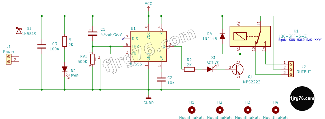
To understand how it works we must remember how the 555 timer works.
The 555 timer and its memory effect
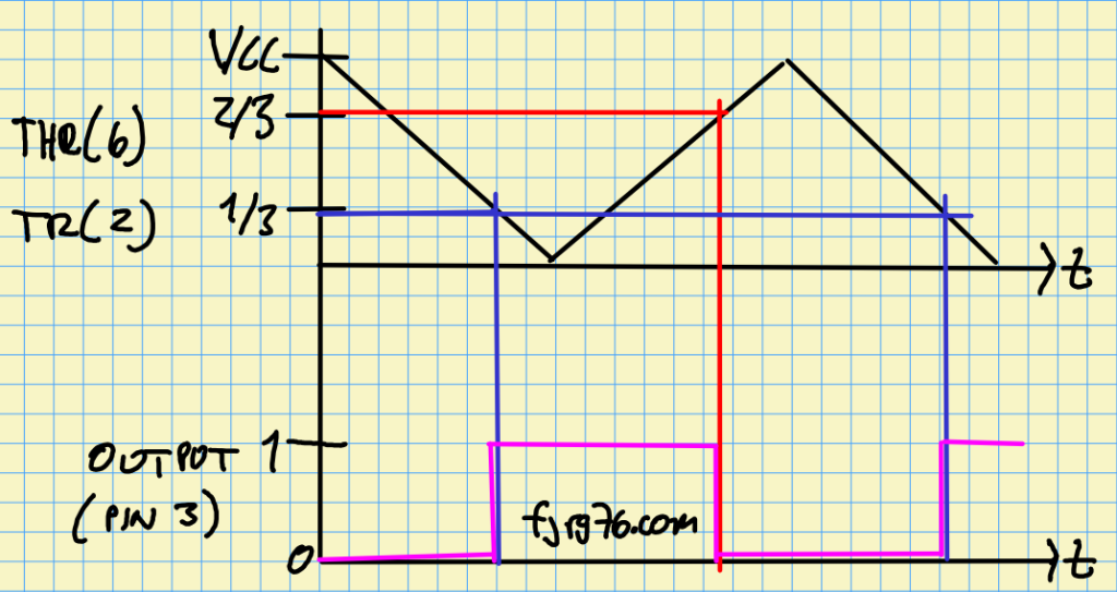
Let’s start by looking at the conditions that the 555 timer must meet for needs to turn its output on or off.
- To activate its output a voltage below 1/3 of the supply voltage needs to be applied in its terminal 2, TR(igger). For example, if we are supplying the circuit with 12V (VCC=12V), then any voltage below 4V will cause the output (pin 3) to go high. And thanks to the 555 timer’s flip-flop (1-bit memory), the output will stay high until something happens on pin 6, THR(eshold).
- To deactivate the 555 timer’s output a voltage above 2/3 of the supply needs to be applied to its terminal 6, THR(eshold). For example, if we are supplying the circuit with 12V (VCC=12V), then any voltage above 8V will cause the output (pin 3) to go low. And thanks to the 555 timer’s flip-flop (1-bit memory), the output will stay low until something happens on pin 2, TR(igger).
How does the delay work?
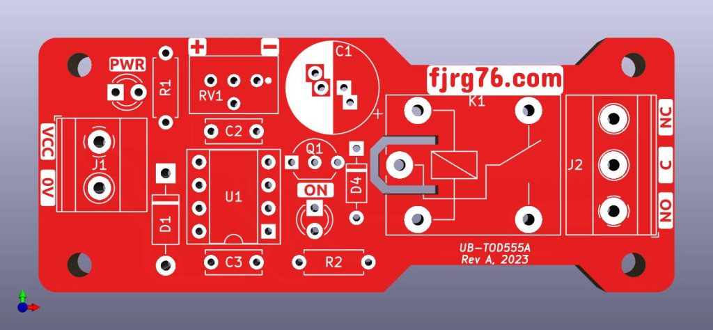
From the schematic note that terminals 2 and 6 (TR and THR) form a node between them and a RC network (C1 and RV1). This means that both inputs are receiving the same voltage at the same time and it will be the value of this voltage that determines if the output goes high or low.
Such control voltage comes from the node with the (-) terminal of the capacitor C1 and one terminal of the potentiometer RV1. And here comes the magic: when the power is supplied to the circuit (at J1) both pins 2 and 6 of the 555 receive VCC volts, which means that the output goes low.
Then C1 begins to charge through RV1, and as this happens the voltage at its (-) terminal begins to slowly decrease, approaching 0V. When the voltage at this terminal drops below 1/3 VDC, then the output goes high, the relay contacts close, and the load is activated. Simple as that.
It was very smart to have placed the capacitor at the top of the RC network as this ensures that its (-) terminal will always receive VCC volts when power is applied to the circuit.
Why does the capacitor’s (-) terminal receives VCC volts when you first apply voltage?
I’ve just explained it in the intro: a discharged capacitor behaves as a short circuit, so when VCC volts are applied on its (+) terminal, then the (-) terminal also receives VCC. This condition changes as the capacitor charges. In this application the short circuit is good; in other applications it can be terrible.
Variant (to avoid cold starts)
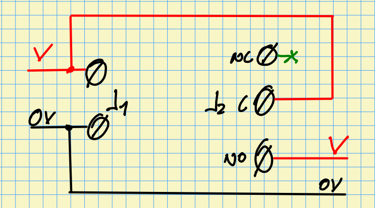
In the circuit that I have presented you can connect anything to the output terminals; however, for the application where we want to avoid cold starts (to delay the arrival of VCC to our circuit) we need to wire VCC to the C(ommon) terminal of the relay, and wire VCC to the NO (Normally Open) terminal:
Chinese timer issues
The Chinese timer implementation has many issues::
- C1 and RV1 are fixed; even worse:
- RV1 is a multiturn potentiometer preset type and there is no visual indication for the chosen delay time, so you will have to use trial and error.
- You can’t easily replace RV1 because two of its terminals are soldered to a copper pad (ground plane on the underside) which requires a lot of heat to melt the tin.
- There is no air gap between the C(ommon) terminal and the relay coil terminals. Depending on the connected load, electric arcs or charring could occur. Worse yet, the bottom ground plane is dangerously close to the C(ommon) high voltage terminal.
- The tracks from the relay terminals (NO, C and NC) to the output connector are too thin to support 10A or 15A. The anti-solder mask was also applied onto them, which prevents you from reinforcing them with extra tin.
- The output connector cannot accept large gauge wire or cable (for holding up to 10A/15A).
- The relay’s coil is for 12VDC and therefore the circuit power (VCC) must also be 12VDC. Imagine that your final application uses 5 or 6 or 9 or 15VDC as activation voltage; in such cases this board will not work for you.
- If you need longer delay times you should change capacitor C1 for a larger one; and the larger the capacitor, the greater will be both its volume and the distance between its terminals. This card is not prepared for that.
How all this issues were solved?
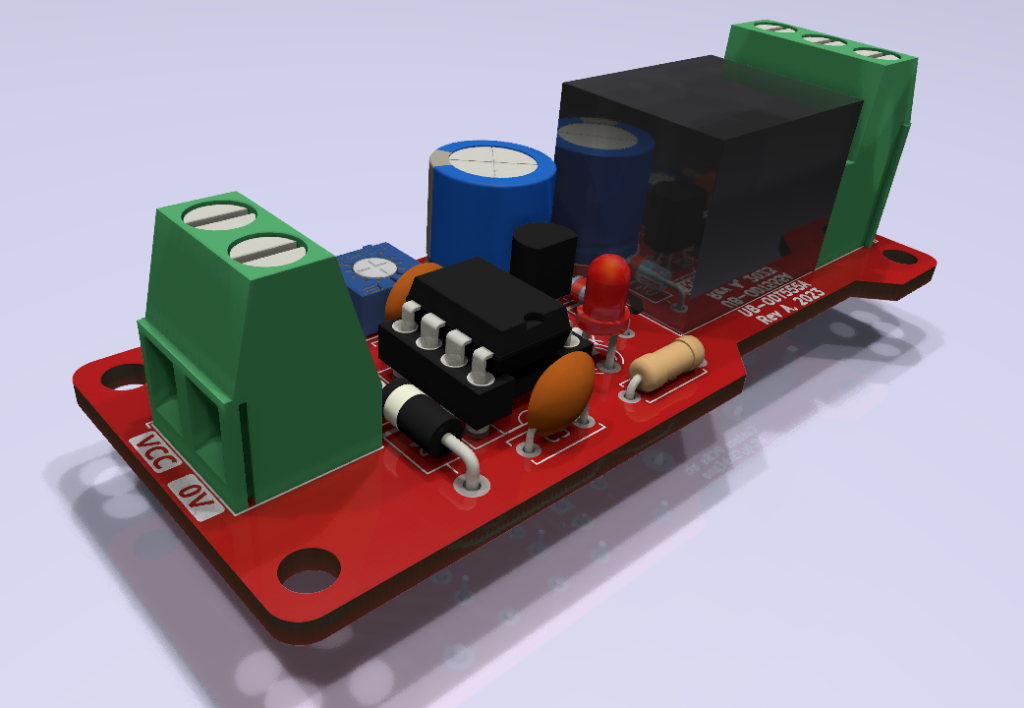
I designed my own printed circuit board (PCB) thinking about my own needs (and yours, of course) avoiding all the issues that I’ve just showed you. Even better, I’ve designed two versions, one for homemade and one for professional production. In any case:
- I designed the PCBs with Through-hole components and single-sided PCB so we can build it ourselves in our labs.
- I used a single turn potentiometer that can easily and visually show the delay time. And in case you can’t get this type of potentiometer, or you don’t like it, then you can still use the multi-turn preset. The PCB is prepared to receive both.
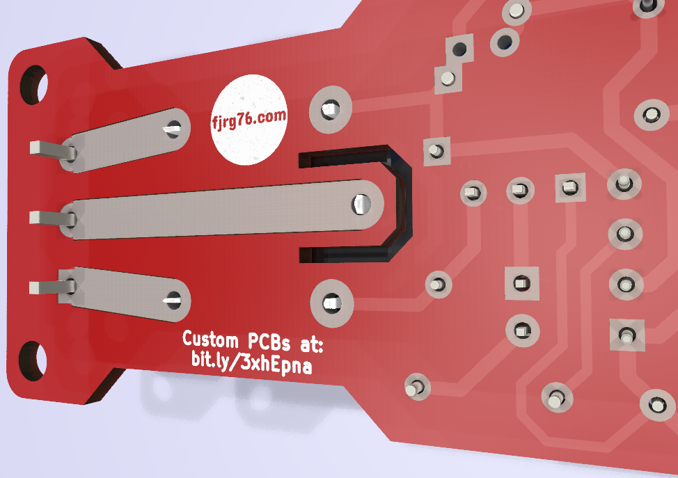
- The professional version includes an internal slot for protection against electric arcs and carbonisation on the C(common) and relay coil (K1) terminals.
- The relay tracks are ready to receive extra tin to help the circuit handle large currents. In extreme cases you could even solder a piece of copper.
- If you need very long delays, in addition to changing the value of the potentiometer at will, you can also place large value capacitors. There is plenty of space and, very importantly, the design supports two distances for its terminals.
- You decide the coil voltage for the relay; that is, according to your needs (not mine) you can choose the supply voltage, from 5VDC to 15VDC.
- You can choose between different output connectors.
- PCB dimensions and mounting holes use integer values so you can set up your mounting base very easily.
- The version for professional manufacturing is visually more attractive.
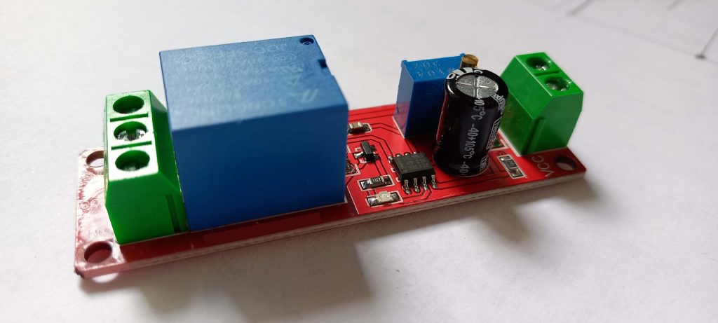
- It is very compact: it measures only 71mm x 22mm.
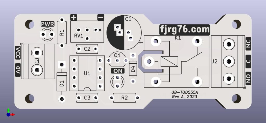
The version for professional manufacturing:
- Includes an internal air gap (internal slot) to prevent arcing and charring.
- The relay leads allow tin to be added as reinforcement for large currents.
- The external cut makes it look more attractive.
Differences between the home-made version and the professional one
Homemade manufacturing
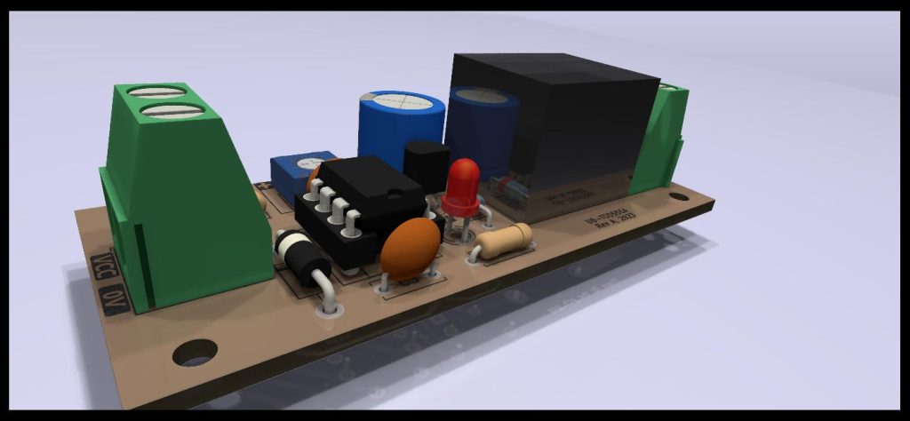
You can build this board at home with the classic tools and completely free of charge:
- Laser printer.
- Iron for toner transfer.
- Ferric acid for copper etching.
- Homemade drill for perforations.
- Etc.
And if you wish, you can add the top silkscreen layer (the procedure is the same as that of transferring the tracks to copper.)
This version is functionally identical to the professionally made version, except for the internal slot, extra cutouts, and eventually the top silkscreen.
To obtain the design click on the following link. After registering you will be receiving a 1:1 scale PDF document so you can make your own cards.
Professional manufacturing
This version is identical to the homemade one, but it includes an internal cut, solder mask (except on relay output tracks), silkscreen overlay, and cutouts that make it look aesthetically pleasing.
Characteristics
You can also choose between different colors and get as many as you want.
Take into account that this version should be manufactured in a professional house. But don’t panic, there’s good news: PCBWay is a serious, high-quality manufacturer whose prices start at $5 for 10 cards. Of course you can order many more, if you require it. If you are not in a hurry and are willing to wait a few weeks, then you can choose a super cheap shipping method.
If you opt for this version, or you liked the circuit but you don’t know how to make your own boards, then click on the following button which, after the registration process, will take you to the PCBWay project page. Once there you can order the cards directly.
Final words
The 555 timer is one of the simplest and most versatile ICs out there. Today I’ve showed you a very interesting application (I have many more that I will be documenting). While that happens, you can see other uses of this chip on my YouTube channel.
Drop me a line if you built this project, if it was difficult for you or in which applications you are thinking of. See you in a next article.


Mi perfil completo lo puede encontrar en: https://www.linkedin.com/in/fjrg76-dot-com/
- Arduino and ESP32 whims - diciembre 17, 2025
- Writing Scalable Firmware: Implementing the Command Pattern in C++ - diciembre 4, 2025
- Patrón de diseño de software Command para sistemas embebidos para los no iniciados - noviembre 30, 2025
Deja una respuesta
Lo siento, debes estar conectado para publicar un comentario.